High-resolution scanning probe microscopy
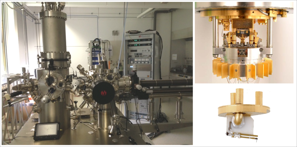
Our investigations use a surface science approach to study atomically defined model systems in ultra-high vacuum to obtain a fundamental understanding of the surface physics/chemistry of low-dimensional and molecular materials. Our main characterization is based on high-resolution scanning probe microscopy techniques, including derived spectroscopic methods, in ultra-high vacuum and at low temperatures (4K). The simultaneous combination of several scanning probe methods (scanning tunneling and force microscopy, STM, and nc-AFM) is a well-established and powerful tool for determining the geometric and electronic structure of surfaces and nanomaterials down to a single chemical bond. AFM is more geometry sensitive, while STM/STS probes the electronic density of a material. Therefore, we can combine an unprecedented spatial resolution down to a single atomic bond with the study of the related electronic structure of the materials. In addition, scanning probe techniques allow tracking complex on-surface chemical reactions, investigation of novel reaction products, and even synthesizing new structures one bond at a time via tip-indued manipulation. The Maier group has extensive expertise in scanning probe methods and has two well-equipped microscopes to perform state-of-the-art high-resolution experiments at low temperatures.
In addition, we use low-energy electron diffraction (LEED) and Auger electron spectroscopy (AES) as complementary surface characterization tools. LEED is a traditional surface science technique to examine the crystallinity and long-range order of a given surface. AES is a common technique for determining the elemental composition of solid surfaces. With AES, we can overcome the lack of chemical sensitivity in SPM.
 |
 |